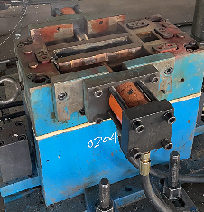
Semiconductor gaskets serve as vital components in microelectronics production, providing precision sealing and spacing in wafer processing, chip packaging, and testing environments. These components demand exceptional dimensional accuracy, surface finish, and chemical resistance to maintain the integrity of sensitive semiconductor processes. The molds used to manufacture these gaskets play a decisive role in ensuring consistent quality, as even micrometer-scale deviations can compromise sealing performance or introduce particulate contamination. High-purity steel has emerged as the material of choice for semiconductor gasket molds, offering the unique combination of mechanical stability, chemical inertness, and ultra-precision manufacturing capabilities required in this critical industry sector.
Material Selection for Semiconductor Gasket Molds: High-Purity Steel Properties and Advantages
The semiconductor industry’s stringent requirements necessitate specialized mold materials that exceed standard industrial specifications. High-purity mold steel, particularly grades formulated for ultra-clean applications, provides four key advantages:
Ultra-low impurity content is paramount, with sulfur and phosphorus levels typically controlled below 0.005% to prevent micro-porosity and particle generation during molding. These steels undergo specialized refining processes such as Electro-Slag Remelting (ESR) to eliminate inclusions that could compromise surface finish or introduce contaminants into the semiconductor environment.
Superior wear resistance ensures molds can maintain nanometer-level surface roughness(Ra ≤ 0.01 μm) over extended production runs. Through precise heat treatment, these steels achieve hardness levels of 50-55 HRC while maintaining toughness, resisting micro-cracking during the high-pressure molding of engineered polymers like PEEK and PTFE composites.
Chemical inertness protect mold from degradation in contact with aggressive cleaning agents and process chemicals. Passivation treatments create a uniform chromium oxide layer, providing resistance to nitric acid, hydrofluoric acid, and other corrosive substances common in semiconductor manufacturing environments.
Dimensional stability under thermal cycling prevents mold distortion during the molding process. Advanced alloying elements like vanadium and niobium minimize thermal expansion coefficients, ensuring critical dimensions remain within ±0.5 μm tolerance even when exposed to temperature fluctuations between 20°C and 180°C.
Precision Design and Manufacturing Technologies for Semiconductor Gasket Molds
Semiconductor gasket mold design requires a holistic approach to precision engineering, encompassing macro-scale structure and nano-scale surface characteristics. Computer-Aided Engineering (CAE) simulations optimize mold cavity geometry, accounting for polymer shrinkage rates as low as 0.1% for specialized semiconductor materials.
Micro-feature replication demands advanced machining technologies:
- Ultra-precision CNC milling achieves positional accuracy of ±1 μm using diamond-tipped tools
- Electron Beam Lithography (EBL) creates sub-micron surface textures for controlled release properties
- Focused Ion Beam (FIB) machining produces complex gasket sealing lips with radius tolerances of ±0.5 μm
Cooling system design is critical for maintaining temperature uniformity within ±0.5°C across the mold surface. Conformal cooling channels, produced via additive manufacturing or laser drilling, ensure consistent solidification of molten polymer, reducing residual stresses that could distort gasket sealing surfaces.
Surface engineering processes include:
- Plasma electrolytic polishing to achieve mirror finishes with Ra < 0.005 μm
- Chemical vapor deposition of diamond-like carbon (DLC) coatings for enhanced wear resistance
- Photo-induced hydrophilic treatment to prevent static charge accumulation and particle adhesion
Quality Control and Clean Manufacturing Standards of Semiconductor Gasket Mold
Semiconductor gasket mold production operates within stringent quality frameworks that exceed typical industrial standards:
Cleanroom manufacturing environments (ISO 14644 Class 5) prevent particulate contamination during all stages of mold fabrication. Airborne particle counts are maintained below 35 particles (>0.5 μm) per cubic meter, with dedicated gowning protocols and filtered ventilation systems.
Metrological verification employs multi-sensor coordinate measuring machines (CMM) with uncertainty values as low as U95=0.3 μm + L/1000. Optical interferometry systems verify surface flatness across the mold cavity to within 0.1 μm over 100 mm lengths.
Material certification requires comprehensive chemical analysis, including:
- Gas chromatography-mass spectrometry (GC-MS) for volatile organic compound testing
- Inductively coupled plasma mass spectrometry (ICP-MS) for trace element analysis (detection limits down to 1 ppb)
- Metallographic examination to ensure inclusion ratings meet SEP 1920 Class 2 requirements
Process validation involves molding qualification coupons under production conditions, with 100% inspection using automated optical inspection (AOI) systems capable of detecting 0.5 μm defects on transparent materials.
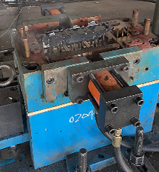
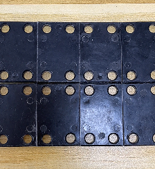
Application-Specific Semiconductor Gasket Mold Solutions for Semiconductor Gaskets
Semiconductor manufacturing encompasses diverse processes, each demanding specialized gasket solutions and corresponding mold technologies:
Wafer handling systems utilize molds for ultra-thin (50-200 μm) polyimide gaskets with micro-grooved sealing surfaces. These molds incorporate precision alignment features to ensure gasket-to-carrier positional accuracy of ±3 μm, critical for wafer centering in lithography tools.
Chip packaging applications require molds capable of producing gaskets with complex 3D geometries for flip-chip and wafer-level packaging. Stacked mold technologies enable integrated sealing and venting features, eliminating secondary operations and reducing particulate generation risks.
Test and inspection equipment relies on molds for conductive gaskets that maintain electrical continuity while providing environmental sealing. These molds feature micro-structured surfaces that control the compression set characteristics of silicone and fluoropolymer materials, ensuring consistent performance over 10,000+ mating cycles.
Maintenance protocols for these specialized molds include:
- Ultra-pure deionized water cleaning with megasonic agitation
- Laser-induced breakdown spectroscopy (LIBS) for contamination mapping-regular nano-indentation testing to monitor surface hardness degradation
Conclusion
High-purity steel molds represent an enabling technology for semiconductor gasket manufacturing, directly contributing to the industry’s relentless pursuit of miniaturization and reliability. As chip feature sizes shrink below 2 nm and manufacturing environments become increasingly demanding, the precision, cleanliness, and durability of mold systems grow ever more critical.
These specialized mold bridge the gap between macro-scale manufacturing and nano-scale device requirements, embodying the pinnacle of precision engineering. Through continuous innovation in materials science, machining technology, and quality control, steel semiconductor gasket molds will remain indispensable to advancing semiconductor technology and ensuring the integrity of microelectronics that power modern computing and communications.
Frequently Asked Questions of Semiconductor Gasket Mold
What distinguishes semiconductor gasket molds from standard industrial molds?
Semiconductor gasket molds require nano-scale surface finishes (Ra ≤ 0.01 μm), ultra-low particle generation, and chemical resistance to process chemicals, exceeding typical industrial mold specifications by one to two orders of magnitude.
Why is high-purity steel preferred over other materials for these molds?
High-purity steel offers superior dimensional stability, wear resistance, and cleanability compared to alternatives like ceramics or polymers. Its ability to maintain precision over millions of cycles makes it economically viable despite higher initial costs.
How are these molds cleaned and maintained in semiconductor facilities?
Maintenance involves ultra-pure water ultrasonic cleaning, laser-induced contamination detection, and periodic nano-polishing. All procedures are performed in ISO Class 5 cleanrooms to prevent particulate introduction.
What tolerance levels are achievable with semiconductor gasket molds?
State-of-the-art molds routinely achieve dimensional tolerances of ±1 μm, with critical sealing surfaces maintained within ±0.5 μm and flatness deviations below 0.1 μm/m.
Are steel molds compatible with all semiconductor gasket materials?
Yes, properly designed steel molds accommodate all common gasket materials including PTFE composites, liquid crystal polymers (LCP), and perfluoroelastomers, with surface treatments tailored to each material’s release characteristics.